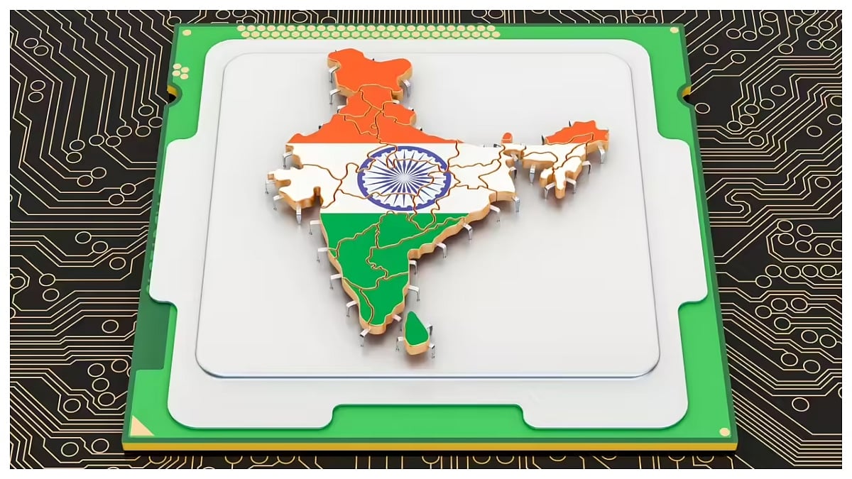
New Delhi: The world is projected to face a shortage of one million semiconductor professionals by 2030 and India has the opportunity to bridge a significant part of this gap, according to Minister of Electronics and IT, Ashwini Vaishnaw.
Highlighting the importance of developing a strong talent base, the minister said that one of the major objectives of the India Semiconductor Mission (ISM) is to create a global pipeline of skilled professionals.

Speaking at the launch of India’s first end-to-end Semiconductor OSAT Pilot Line Facility of CG Power at Sanand, Gujarat, Vaishnaw said the inauguration of the pilot line represents a decisive step in fulfilling Bharat’s dream of developing semiconductor design, manufacturing, and downstream capabilities, with Gujarat emerging as a pivotal hub in this transformation.
Vaishnaw underlined the critical role of the OSAT Pilot Line, noting that chips manufactured here will be used for customer qualification. Once these chips are approved, it becomes much easier for commercial plants to commence full-scale production of qualified products.

He emphasised that this inauguration is among the most significant milestones achieved under the India Semiconductor Mission, which has approved 10 projects so far. The government has also partnered 270 universities and equipped them with state-of-the-art semiconductor design tools.
In 2025 alone, these tools recorded over 1.2 crore usages. As a direct outcome, 20 chips designed by 17 institutions have already been successfully fabricated at the Semi-Conductor Laboratory (SCL), Mohali. The minister stated that very few countries in the world provide students with access to such advanced tools.
He added that this initiative will empower India’s youth, strengthen the technical ecosystem, and position the nation as a global hub of semiconductor talent. The CG Semi facility at Sanand provides end-to-end solutions for chip assembly, packaging, testing and post-test services, covering both traditional and advanced packaging technologies. This marks a major step in strengthening India’s semiconductor capabilities and supporting the country’s goal of becoming self-reliant while also serving global markets.
Disclaimer: This story is from the syndicated feed. Nothing has changed except the headline.