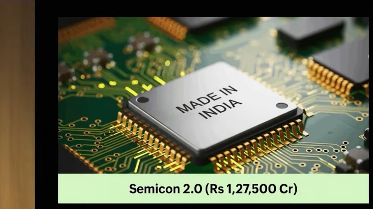
New Delhi: The Union Cabinet on Wednesday approved the Semicon 2.0 long-term policy that seeks to support the design and manufacturing ecosystem for development of semiconductors in India. It provided a total budget outlay of ₹127,500 cr for the scheme that is aimed to develop the semiconductor ecosystem on a “six pillars” concept – covering design, machines and materials, setting up of more fabs, research and development, and talent development.
Following on the success of Semicon 1.0 under which 12 manufacturing units have been approved with a cumulative investment of over Rs. 1.64 lakh crore, the Semicon 2.0 seeks to take the work forward in all essential areas.
The Cabinet said 105 startups have already started developing chips and the focus now is on deepening the design ecosystem. Building blocks have been identified for the development of strategic and commercial products and under Semicon 2.0 the aim is to develop IPs, designs of chips and systems with this approach.
The policy framework would also support manufacturing and R&D of the machines and manufacturing of materials, chemicals and gases that are essential for manufacturing semiconductors. This would help in promoting the precision manufacturing industry in the country.
On setting up of more fabs, the Cabinet said the first fab is scheduled to be commissioned in 2028 and efforts would be made to attract more manufacturers working on silicon fabs, compound semiconductor fabs, discrete component fabs and display fabs among others.
Also Watch:
On promotion to R&D, it said the semiconductor journey began with 28nm-110nm as the node and now the focus would be on developing more advanced nodes and other advanced technologies.
The scheme also seeks to promote talent development. While 315 universities are already training students on complex chip design using the latest EDA tools and 68,000 students have been imparted knowledge, the level of training in colleges would be deepened to cover clean room, fab construction and other ecosystem training as well.